Optimizing the soldering process with tin solder balls is a critical aspect for many industries, including electronics manufacturing, where precision and reliability are of utmost importance. As a trusted supplier of tin solder balls, I’ve witnessed firsthand the transformative impact that well – optimized soldering processes can have on product quality and production efficiency. In this blog, I’ll share some key strategies and best practices to help you get the most out of tin solder balls in your soldering operations. Tin Solder Balls
Understanding the Basics of Tin Solder Balls
Tin solder balls are small spherical pieces of solder alloy, typically made of tin with other metals such as silver, copper, or bismuth added to enhance specific properties. These balls are used in a variety of soldering applications, most notably in ball grid array (BGA) and chip scale package (CSP) technologies. The choice of solder ball alloy depends on several factors, including the application requirements, operating conditions, and compatibility with the printed circuit board (PCB) and components.
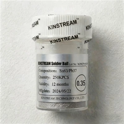
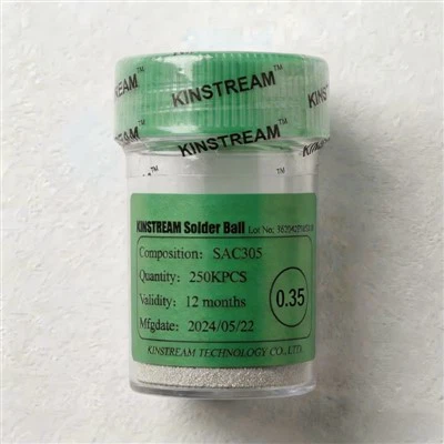
For example, a common alloy is Sn63Pb37, which has a relatively low melting point and good wetting properties. However, due to environmental concerns, lead – free solder alloys like Sn96.5Ag3.0Cu0.5 (SAC305) have become more popular in recent years. Understanding the characteristics of different solder ball alloys is the first step in optimizing the soldering process.
Selecting the Right Solder Ball Size
The size of the tin solder balls plays a crucial role in the soldering process. Smaller solder balls are used for high – density applications where fine pitch components are involved. For instance, in modern smartphones and other compact electronic devices, solder balls with diameters as small as 0.1mm or even less may be used. On the other hand, larger solder balls are suitable for applications that require higher mechanical strength and better heat dissipation, such as power electronics.
When selecting the solder ball size, it’s important to consider the pitch of the component pads on the PCB. The pitch is the distance between the centers of adjacent pads. The solder ball diameter should be chosen such that it can form a reliable connection between the component and the PCB without bridging adjacent pads. A general rule of thumb is that the solder ball diameter should be approximately 70 – 80% of the pad diameter.
Optimizing the Solder Paste Application
Solder paste is often used in conjunction with tin solder balls to facilitate the soldering process. The solder paste contains flux, which helps to clean the surfaces of the PCB pads and the component leads, and also promotes wetting of the solder. The application of solder paste must be precise to ensure consistent soldering results.
One of the key factors in solder paste application is the stencil design. The stencil is a thin metal sheet with openings corresponding to the PCB pads. The thickness and aperture size of the stencil determine the amount of solder paste deposited on each pad. A well – designed stencil will ensure that the right amount of solder paste is applied, neither too much (which can lead to bridging) nor too little (which can result in poor wetting and weak joints).
Another important aspect is the printing process. The solder paste should be evenly distributed across the stencil, and the squeegee pressure and speed should be carefully controlled. Automated stencil printers are commonly used in high – volume production to ensure repeatability and accuracy.
Reflow Soldering Process Optimization
Reflow soldering is the most common method used to melt the tin solder balls and form the solder joints. The reflow process involves heating the PCB and components to a specific temperature profile, which typically consists of a pre – heat stage, a soak stage, a reflow stage, and a cooling stage.
During the pre – heat stage, the temperature is gradually increased to remove any moisture from the PCB and components and to activate the flux in the solder paste. The soak stage helps to ensure uniform heating across the PCB and to further activate the flux. In the reflow stage, the temperature is raised above the melting point of the solder alloy, allowing the solder balls to melt and form a metallurgical bond with the PCB pads and component leads. Finally, the cooling stage is crucial for the formation of a strong and reliable solder joint.
To optimize the reflow process, it’s important to carefully control the temperature profile. This can be achieved by using a reflow oven with precise temperature control capabilities. The temperature profile should be tailored to the specific solder alloy and component requirements. For example, lead – free solder alloys generally require higher reflow temperatures compared to lead – containing alloys.
Inspection and Quality Control
Inspection is an essential part of the soldering process to ensure the quality of the solder joints. Visual inspection can be used to detect obvious defects such as bridging, tombstoning, and insufficient wetting. However, for more accurate and detailed inspection, techniques such as X – ray inspection and automated optical inspection (AOI) are often used.
X – ray inspection can detect internal defects such as voids in the solder joints, which can affect the reliability of the solder connection. AOI uses cameras and image processing algorithms to detect surface defects and ensure that the solder joints meet the required quality standards.
Regular quality control checks should be carried out throughout the production process to identify and correct any issues early on. This can help to reduce scrap rates and improve overall production efficiency.
Troubleshooting Common Soldering Issues
Even with careful optimization, soldering issues can still occur. Some common problems include bridging, tombstoning, and poor wetting.
Bridging occurs when the solder connects two adjacent pads, causing a short circuit. This can be caused by excessive solder paste, improper stencil design, or incorrect reflow temperature. To prevent bridging, it’s important to ensure that the correct amount of solder paste is applied and that the reflow process is properly controlled.
Tombstoning is a phenomenon where one end of a component is lifted off the PCB during the soldering process. This is usually caused by uneven heating or differences in the wetting properties of the solder on the two ends of the component. To prevent tombstoning, the reflow temperature profile should be adjusted to ensure uniform heating, and the component placement should be accurate.
Poor wetting occurs when the solder does not spread evenly over the PCB pads and component leads. This can be due to contaminated surfaces, improper flux activation, or incorrect solder alloy selection. To improve wetting, the surfaces should be properly cleaned before soldering, and the flux should be activated correctly during the reflow process.
Conclusion
Optimizing the soldering process with tin solder balls is a complex but rewarding task. By understanding the basics of tin solder balls, selecting the right size and alloy, optimizing the solder paste application and reflow process, and implementing effective inspection and quality control measures, you can achieve high – quality solder joints and improve the overall performance of your products.
CCGA Solder Column As a supplier of tin solder balls, I’m committed to providing high – quality products and technical support to help you optimize your soldering processes. If you’re interested in learning more about our tin solder balls or have any questions regarding the soldering process, I encourage you to reach out to me for a procurement discussion. We can work together to find the best solutions for your specific needs.
References
- "Fundamentals of Soldering Technology" by John H. Lau
- "Surface Mount Technology: Principles and Practice" by C. P. Wong
Kinstream Technology Co., Ltd.
We’re well-known as one of the leading tin solder balls manufacturers and suppliers in China. We warmly welcome you to wholesale bulk high quality tin solder balls in stock here from our factory. If you have any enquiry about customized service, please feel free to email us.
Address: Room 311, Bldg., 7D, Hengda Shishang Huigu, Dalang Street, Longhua District, Shenzhen, China
E-mail: valuemaxau@163.com
WebSite: https://www.kinstreamspheres.com/